

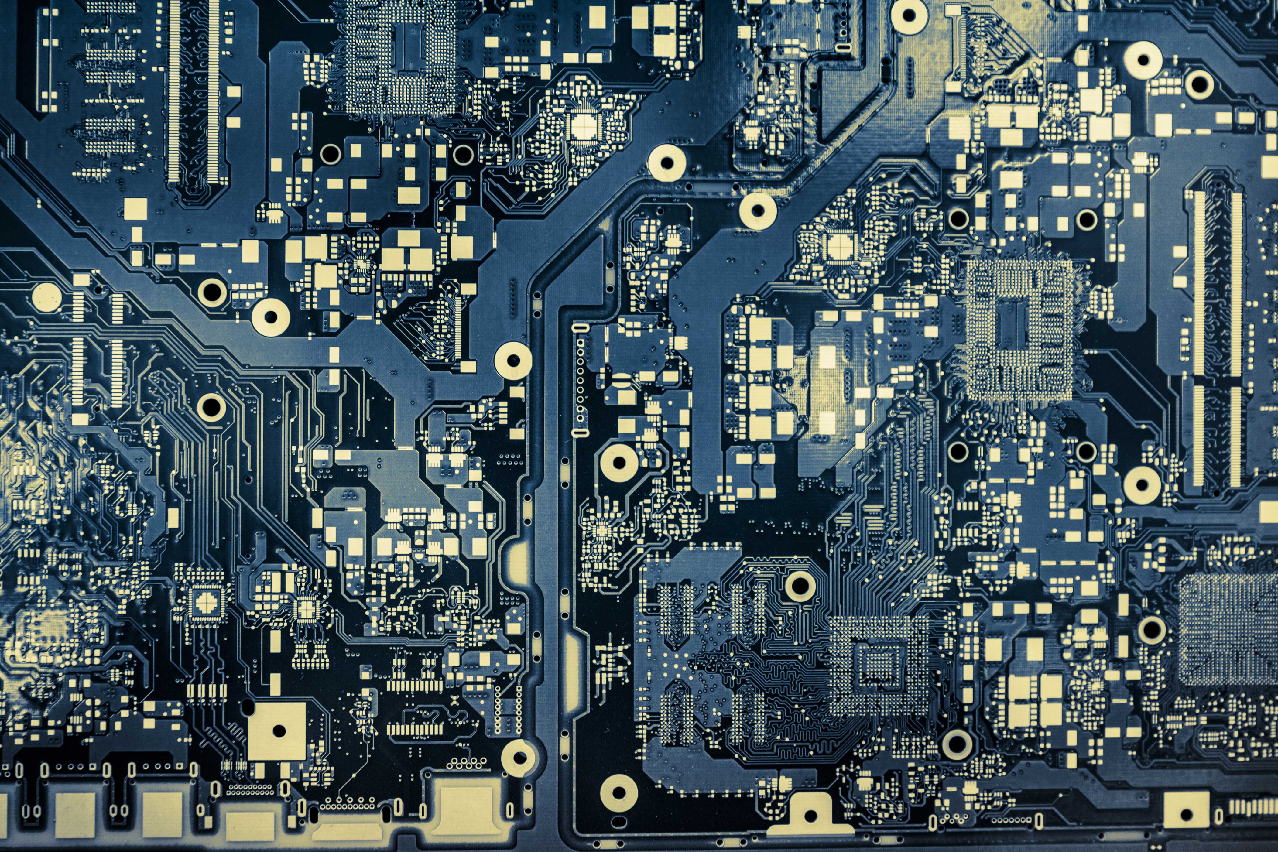
In the electronics industry, electroless nickel electroless gold (ENIG) or electroless nickel electroless palladium electroless gold (ENEPIG) are important corrosion-free high-end surface finishes for coated printed circuit boards. When measuring coating thickness using an instrument with DPP+ digital pulse processor and polycapillaries, it is shown that the measurement time can be significantly reduced without sacrificing measurement precision. Due to its high conductivity and moderate cost, copper is the preferred material in PCB technology. Chemical reactions with the atmosphere or unprotected handling lead to uncontrolled aging effects of the copper surface. For this reason, making an electrical contact directly on copper, for example by soldering, is not process safe. Surface coatings over the current-carrying copper layer have been developed as a solution.
Traditionally, X-ray fluorescence devices have been used in the electronics industry, especially in printed circuit board technology, for non-destructive quality control. IPC-4552B and IPC-4556A are designed to measure spots up to 0.6 mm in diameter. Traditionally, this measurement task was solved with collimator devices. However, the requirements for coating systems are constantly increasing: coatings are becoming more complex, thinner and applied to smaller samples, so that measurement spots with a size of less than 0.3 mm are required in electroplating, for example.
Read the full article in mo issue 11/2022 or online here!