

Layer systems in electronics
Electroless nickel alloys as important corrosion-free high-end surface finishes

Quality inspection is becoming increasingly important in industrial production. Highly complex coating systems and component geometries as well as the required precision of the measurement results and the shortest possible duration of the measurement provide a constant pressure to innovate. This also applies to the electronics industry.
In the electronics industry, electroless nickel electroless gold (ENIG) or electroless nickel electroless palladium electroless gold (ENEPIG) are important corrosion-free high-end surface finishes for coated printed circuit boards. When measuring coating thickness using an instrument with DPP+ digital pulse processor and polycapillaries, it is shown that the measurement time can be significantly reduced without sacrificing measurement precision. Due to its high conductivity and moderate cost, copper is the preferred material in PCB technology. Chemical reactions with the atmosphere or unprotected handling lead to uncontrolled aging effects of the copper surface. For this reason, making an electrical contact directly on copper, for example by soldering, is not process safe. Surface coatings over the current-carrying copper layer have been developed as a solution.
Electroless nickel immersion gold (ENIG or Electroless Nickel Immersion Gold) and electroless nickel immersion palladium immersion gold (ENEPIG or Electroless Nickel Electroless Palladium Immersion Gold ) are important corrosion-free high-end surface finishes for highly reliable electrical contacts and bond connections, respectively. The thickness of the individual gold (Au), palladium (Pd) and electroless nickel layers is crucial for their optimum function and durability. Precise control of these layers is therefore crucial. The gold layer thickness is relevant for the contact resistance, while the palladium layer serves as a diffusion barrier and contributes to the optimization of the bonding properties. The ENEPIG palladium layer also prevents a so-called brown powder effect from occurring, in which a brown contact layer forms and causes high contact resistance. This can be a problem with ENIG. The simultaneous minimization of material costs for the gold and palladium coatings are an aspect that should not be neglected for economic reasons - especially due to the increased raw material prices for precious metals.
(Kopie 3)
Standards and metrology
The global electronics manufacturing association IPC published the latest version of the IPC-4552 (ENIG /PCB) standard in 2021 as IPC-4552B. This specifies the requirements for the coating thickness of ENIG in applications such as soldering, wire bonding, and as a contact surface. It specifies the amount of gold applied to optimize product performance. Accurate quality control of the gold layer thickness is required for this purpose. According to IPC-4552B and IPC-4556A, proof of suitable quality control must be ensured by measuring equipment analysis. IPC-4552B (for ENIG) and IPC-4556A (for ENEPIG) thus define the requirements for measuring devices for checking the layer thickness. IPC-4552B now also allows Reduction Assisted Immersion Gold (RAI Gold). ENIG deposition with RAI Gold meets the highest rating in terms of coating durability according to the IPC-J-STD-003 specification for PCB solderability.
Traditionally, the electronics industry, especially the printed circuit board industry, has relied on X-ray fluorescence equipment for non-destructive quality control. IPC-4552B and IPC-4556A are designed to measure spots up to 0.6 mm in diameter. Traditionally, this measurement task was solved with collimator devices. However, the requirements for coating systems are constantly increasing: coatings are becoming more complex, thinner and applied to smaller samples, so that, for example in electroplating, measurement spots with a size of less than 0.3 mm are required. More complex component geometries require a greater distance between the measuring device and the sample, and thinner coatings down to the nm range demand the ability to reliably measure very thin layers.

X-ray fluorescence measurement technology in the electronics industry
An alternative that can meet these challenges is optics with so-called polycapillaries. These consist of a system with a large number of hollow capillary channels. Their mode of operation is based on the effect of total external reflection of X-rays from the inner smooth surfaces of the capillary channels, which are made of special glass. This type of optics enables focusing of polychromatic X-rays, i.e. white X-rays. Depending on the application objective, individual parameters of the optics can be optimized. Thus, it is possible to generate small measuring spots below 100 µm with very high intensities.
Measurement of ENIG and ENEPIG
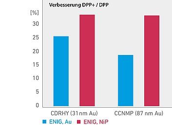
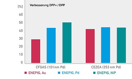
For a comparative analysis, ENIG and ENEPIG calibration standards were measured with regard to the achievable repeatability of the simultaneously measured layer thicknesses at a measurement time of 1...30 seconds. The comparison is based on values measured with the new Fischerscope X-RAYXDV-μ with the advanced digital pulse processor DPP+, and a Fischerscope X-RAY XDV-μ with DPP. The instruments used are each equipped with 50 mm2 silicon drift detectors (SDD), 20-μm halo-free polycapillaries, and tungsten anode X-ray tubes. The performance was determined based on the repeatability precision achieved for both devices and put into perspective. The gain in precision is illustrated in graph 1 for the different samples. An improvement of 50 percent corresponds to a halving of the measurement uncertainty. The comparison shows that the Fischerscope X-RAY XDV-μ with DPP+ has a significantly improved precision for the coating thickness measurement of ENIG and ENEPIG metal structures at a fixed measurement time. An improvement in precision of about 20 to 50 percent can be achieved depending on the layer thickness and the specific application. Thus, typical gold coatings with thicknesses below 100 nm can be measured with a precision of <1 nm in less than ten seconds. Alternatively, with constant precision compared to the predecessor XDV-μ with DPP, the measurement time can be significantly reduced and thus the throughput can be increased accordingly.
The new X-ray fluorescence instrument is ideally suited for quality control in the electronics industry, where electroless nickel immersion gold (ENIG) or electroless nickel immersion palladium immersion gold (ENEPIG) are important corrosion-free high-end solutions for coated printed circuit boards and can be measured quickly and precisely with the XDV-µ.
Helmut Fischer GmbH Institute for Electronics and Measurement
www.helmut-fischer.com