

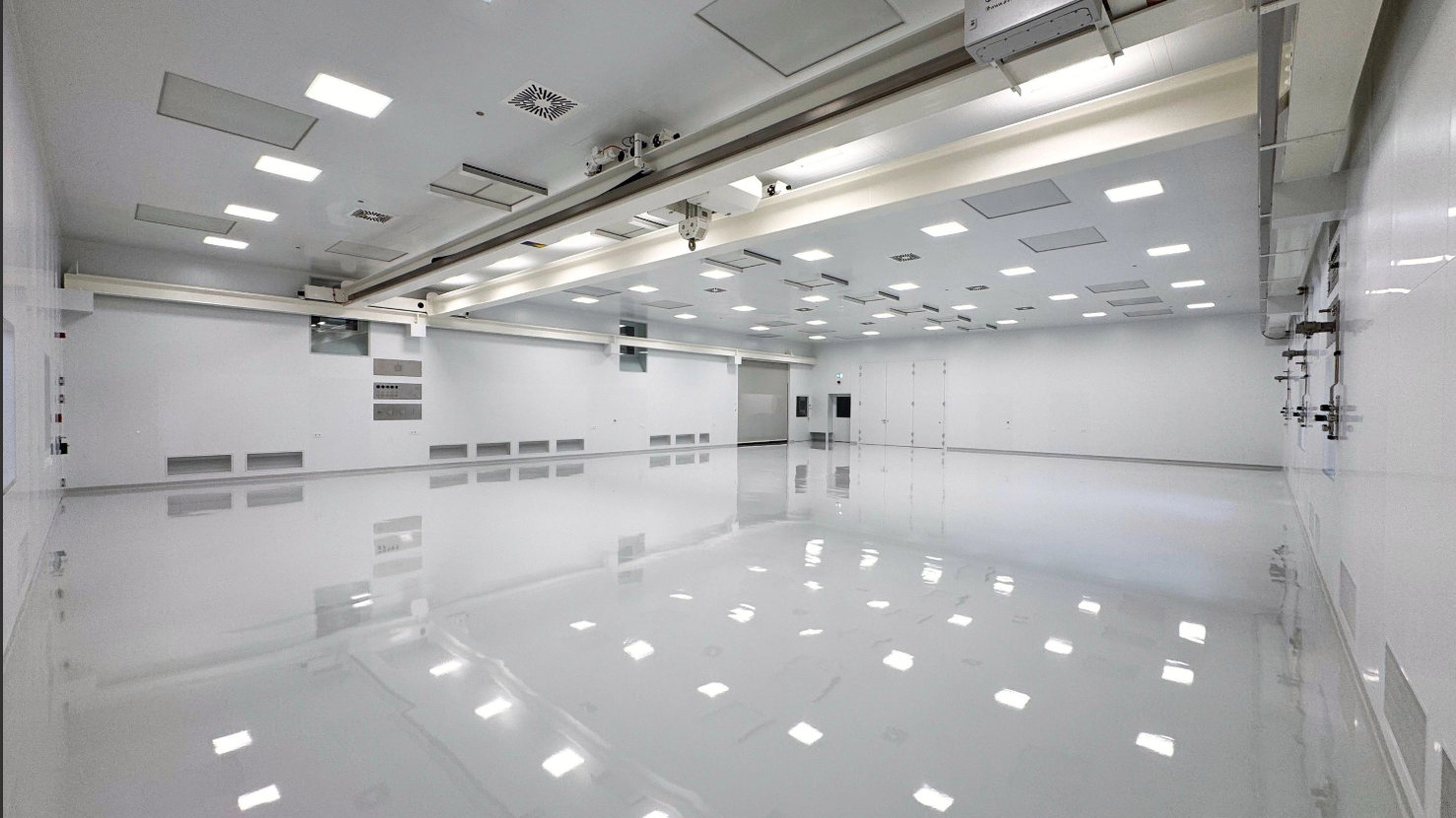
The 700 m² cleanroom has ISO 5 and ISO 7 areas. According to the company, this makes it suitable for process and system development, sampling, system assembly or system operation. It offers optimum conditions to meet the requirements of the semiconductor industry, materials science and medical applications.
Novel semiconductor applications require new materials and their application to drive innovation and push technological boundaries. The company's process and materials expertise is critical to developing and introducing new materials and supporting customers in their process and product development.
Initially, Von Ardenne plans to install its new Opta X300 system platform, which will be available from mid-2026 for both internal and partner development projects. The Dresden-based system manufacturer covers the entire process chain - from the simulation of processes in the system to the simulation of coatings and their functions through to the measurement and evaluation of coating properties.
This gives customers the opportunity to test the function of the coating for their product in the relevant environment in advance. For example, optical coatings and materials for piezoelectric and memory applications are increasingly in demand. The new cleanroom and the equipment installed in it are intended to accelerate the development of such materials.
"We look forward to working with our partners in this state-of-the-art environment and driving innovation in next-generation semiconductor applications," says Sven Frauenstein, VP Semiconductor at Von Ardenne.