

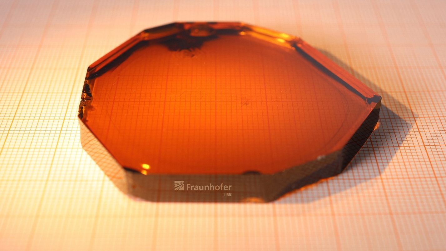
According to PVA Tepla, this will improve the availability of AlN substrates across Europe. In turn, this is expected to accelerate the development of AlN-based devices and systems and their transition into industrial applications. As an ultra-wide-bandgap (UWBG) semiconductor, AlN opens new possibilities in photonics, power electronics, radio-frequency electronics, and electronics designed for extreme operating environments. Until now, the shortage of high-quality, large-area, and cost-effective AlN substrates has slowed the development of AlN-based electronic systems.
New generation of electronic devices
"With the joint lab, we are laying the foundation for a reliable European supply of AlN substrates and creating new opportunities for the next generation of high-performance AlN devices," said Dr. Sven Besendörfer, head of the Nitride Materials Group and responsible for AlN materials development at Fraunhofer IISB. "Together with PVA Tepla, we are contributing our expertise in industrial crystal growth and creating the conditions needed to transfer this technology into practical applications."
At the joint lab, Fraunhofer IISB is using its proprietary Physical Vapor Transport (PVT) process technology to produce 2-inch bulk AlN crystals. In this process, AlN powder is vaporized in a crucible at temperatures well above 2,000°C and deposited onto a seed crystal. PVA Tepla is providing the PVT systems, which are already deployed worldwide for the production of 8-inch silicon carbide (SiC) crystals and have now been adapted for growing 2-inch AlN crystals. Thanks to the process expertise contributed by Fraunhofer IISB, PVA Tepla's team was able to quickly acquire the capability to produce AlN crystals of comparable quality using its own equipment. The joint lab is focused on establishing a stable pilot-scale production of 2-inch AlN crystals. Production is now being ramped up step by step to optimize process stability, reproducibility, yield, and cost structures.
Strengthening Europe through industrial scaling
The AlN crystals produced in the joint lab will be processed into epi-ready AlN substrates at Fraunhofer IISB and transferred into industrial development and scale-up activities through LZE GmbH. "For Europe's semiconductor sovereignty, it is essential not only to develop new key materials but also to rapidly transfer them into industrial applications and scalable value creation. Through its marketplace, LZE GmbH provides companies and research institutions with access to AlN substrates," said Dr. Christian Forster, managing director of the company.
At the same time, Fraunhofer IISB is advancing the development of 4-inch and, in the longer term, 6-inch AlN technology. The joint lab therefore lays the foundation for the medium- to long-term scaling of substrate sizes.