

Piezoelectric materials generate an electrical voltage when they are deformed and deform in return when an electrical voltage is applied. In addition to frequency filters, piezoelectric thin films are used for many other components in microelectronics. Additional applications, such as for quantum technologies, are the subject of ongoing research. In order for such thin films to do their job, they must be of high quality.
Researchers from the Swiss Federal Laboratories for Materials Science and Technology (Empa) in the "Surface Science & Coating Technologies" department have developed a new coating process for piezoelectric thin films. Using their method, the layers can be produced in very high quality on insulating substrates and at a relatively low temperature, as the research institute reports. The researchers have applied for a patent for the process.
Argon must not enter the piezoelectric layer
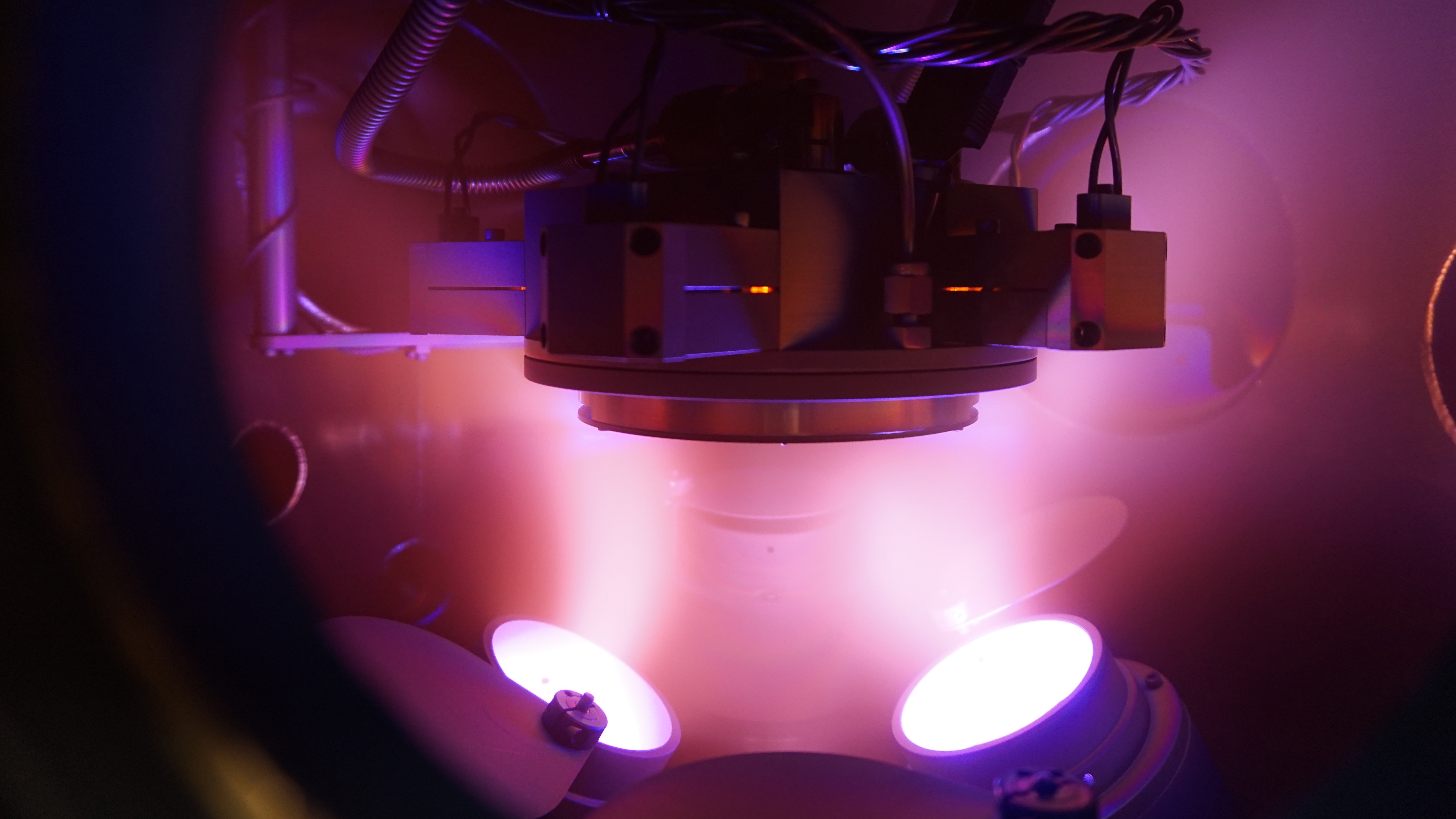
The researchers used the HiPIMS coating process (high-power impulse magnetron sputtering) as a basis. Until now, this process was not suitable for piezoelectric thin films. This is because when a voltage is applied to the substrate, not only are the layer-forming target ions accelerated onto the substrate, but also the argon ions from the process gas. This argon bombardment must be avoided. "Several percent argon can sometimes be trapped in hard material layers," says Empa researcher Sebastian Siol. "High voltages often have to be applied to a piezoelectric thin film. This would lead to a catastrophic electrical breakdown."
Nevertheless, the researchers working with Siol believed in the potential of HiPIMS for piezoelectric thin films. The high energy with which the ions fly towards the substrate is advantageous. If the ion hits the substrate with sufficient energy, it remains mobile on the substrate for a short time and can find an optimal position in the growing crystal lattice. But what can be done about the argon inclusions?
Jyotish Patidar developed a solution as part of his doctoral thesis. Not all ions arrive at their destination at the same time. The majority of argon ions are located in the plasma in front of the target. This means that they often reach the substrate faster than the target ions, which first have to be knocked out of the target and also have to cross the entire distance. Patidar's trick was the timing: "If we apply the voltage to the substrate at exactly the right moment, we only accelerate the desired ions," explains Siol. The argon ions have already flown past at this point - without the additional acceleration, they have too little energy to gain a foothold on the substrate.
"Electron shower" now serves as an air traffic controller
With this trick, the researchers were able to produce high-quality piezoelectric thin films using the HiPIMS process for the first time - equivalent to or even better than with conventional methods. Now came the next challenge: depending on the application, the thin film needs to be produced on an insulating substrate, such as glass or sapphire. However, if the substrate is non-conductive, no voltage can be applied to it. Although there is a way in industry to accelerate the ions anyway, this often leads to argon inclusions in the layer.
This is where the Empa researchers achieved a breakthrough. To accelerate the ions onto the insulating substrate, they use the magnetron pulse itself - the short pulse that shoots the process gas ions onto the target. The plasma in the chamber contains not only ions, but also electrons. Each pulse from the magnetron automatically accelerates these negatively charged elementary particles onto the substrate. The tiny electrons reach their target much faster than the ions.
Normally, this "electron shower" is not relevant for the HiPIMS process. However, when the electrons arrive at the substrate, they give it a negative charge for a fraction of a second - enough to accelerate ions. If the researchers trigger a subsequent magnetron pulse at exactly the right time interval, the electron shower accelerates the target ions that "flew off" during the previous pulse. And, of course, the timing can also be adjusted so that only the right ions end up in the thin film.
Further use of chips for qubits planned
"With our method, we were able to produce piezoelectric thin films on insulating substrates just as well as on conductive ones," summarizes Siol. The researchers call the process "Synchronized Floating Potential HiPIMS", or SFP-HiPIMS for short. This allows piezoelectric thin films to be produced in very high quality at low temperatures. This opens up new possibilities for the production of chips and electronic components, which often cannot withstand temperature extremes. The process for insulating substrates is particularly important for the semiconductor industry: "The processes in semiconductor production are designed in such a way that there is often no possibility of applying an electrical voltage to the substrate," says Siol.
With his research group, he will next focus on the production of ferroelectric thin films - another key technology in today's and future electronics. Based on this success, the Empa researchers are also launching several projects with other research institutions to bring their thin films into applications ranging from photonics to quantum technologies. And finally, they want to further optimize the process with the help of machine learning and high-throughput experiments.
Literature:
J. Patidar, O. Pshyk, K. Thorwarth, L. Sommerhäuser, S. Siol: Low temperature deposition of functional thin films on insulating substrates enabled by selective ion acceleration using synchronized floating potential HiPIMS; Nature Communications (2025); doi: 10.1038/s41467-025-59911-y