
Boron nitride (BN) - also known as "white graphene" - is a layered material consisting of the elements boron (B) and nitrogen (N) and can occur in various forms, including hexagonal boron nitride (hBN). Similar to graphene, hBN has a hexagonal lattice structure and its 2D layers are used in various applications, for example in quantum optics or infrared nanophotonics, or simply as a substrate or encapsulation material. For such applications, a precise characterization of the hBN layers is crucial. However, apart from the resonance in the mid-infrared range, hBN as a single layer is transparent over the entire near-infrared and visible spectral range. Therefore, it cannot be examined with conventional optical microscopes. This property has so far severely limited the use of hBN in the development of new materials. For example, in order to identify possible distortions and material boundaries in 2D layers, these must be imaged precisely. In addition, researchers stack individual layers of 2D materials on top of each other to create van der Waals structures. Ideally, researchers would like to observe this layering under the microscope, also to see the orientation of the individual layers.
Sum frequency microscope makes the hBN layers visible
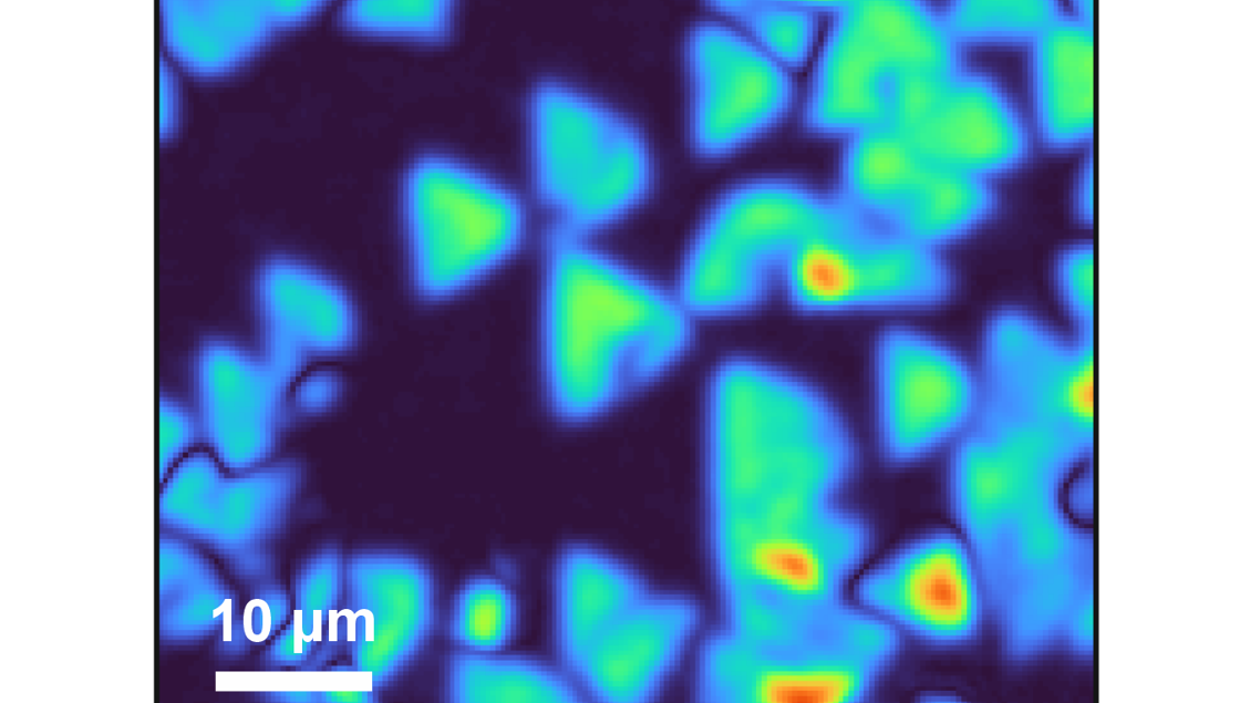
The research team at the Fritz Haber Institute has developed a microscope that uses a trick from non-linear optics to make the otherwise invisible material hBN visible. In their method, phase-resolved sum frequency microscopy, two laser beams, one in the mid-infrared range and one in the visible range, are mixed to generate a sum frequency signal in the sample. By exciting an hBN grating vibration, the sum frequency signal becomes so intense that not only sample areas of 100 × 100 μm2 are imaged in less than 1 s, but even the crystal orientation becomes visible. Thanks to their new microscope, the researchers were able to show that the 2D layers of hBN, which grow in triangular domains, have nitrogen-terminated zigzag edges. In addition, the high nonlinearity in the frequency range of the vibrational resonance underlines that single-layer hBN is a promising material for frequency upconversion - from infrared to visible light - in new optoelectronic devices.
Prospects of the new microscopy method
The newly developed microscope offers advantages over other methods. First and foremost, it can visualize optically transparent materials. The microscope images have a higher contrast than conventional AFM images, and the signal amplification by vibrational resonance enables live imaging of hBN, including online information about its crystal orientation. The new microscope thus enables the controlled production of van der Waals structures.